Electronic Design
High-Performance Electronic Systems Engineered to Your Specifications
Nexilica specializes in designing advanced electronic systems, engineered to precisely meet the technical and functional requirements of businesses in industrial, automotive, IoT, and embedded markets. Every project starts with an in-depth requirements analysis and is developed through a structured engineering process that ensures reliability, scalability, and optimal system integration.
From the electronic board to functional prototyping and firmware development, we manage the entire development cycle in-house.
01 / Competencies
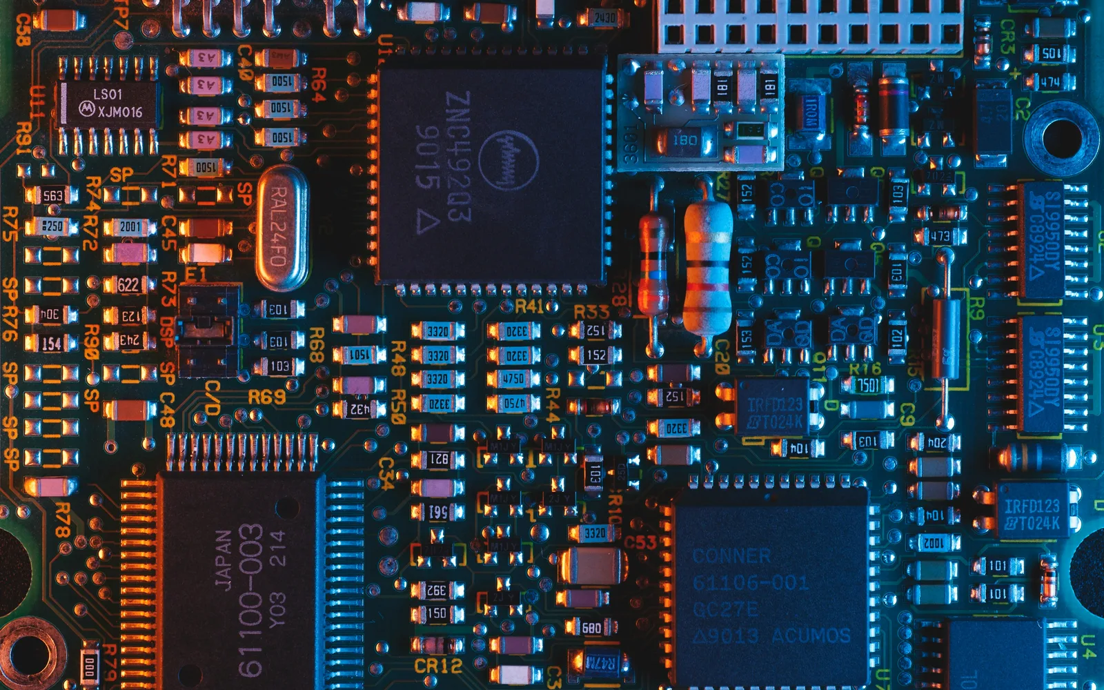
Circuit Design and PCB Layout
The key competencies of this service
02 / Applications
Application Areas
- Industrial automation and control systems
- Automotive and motorsport
- IoT and embedded systems
- Instrumentation and sensor technology
03 / Advantages
The Advantages of Our Electronic Design
04 / FAQ
Electronic Design: Our Customers' Questions
How long does it take to design a custom electronic board?
A standard electronic board design typically takes 2 to 6 weeks from specification to production-ready deliverables. From initial concept to a first working prototype, the timeline is usually 4 to 8 weeks depending on system complexity and component availability.
How does custom electronic board design work?
Custom electronic board design follows a structured process: specification analysis, schematic capture, multilayer PCB layout, simulation and verification, and generation of production files (Gerber, BOM, pick-and-place). Each phase is validated with the client before proceeding, ensuring the final result meets all requirements.
From concept to prototype: what are the stages of electronic board development?
Electronic board development follows a structured path: requirements analysis and feasibility, schematic design, PCB layout, DFM (Design for Manufacturing) verification, prototype production, assembly, functional testing, and validation. At the end, complete technical documentation is delivered for series production.
What technologies are used in industrial electronic design?
Industrial electronic design requires multidisciplinary expertise spanning analog, digital, RF, and power electronics. Common technologies include ARM microcontrollers (STM32, Cortex-M), FPGAs, power converters, industrial communication interfaces (CAN, RS-485, Ethernet), and advanced sensors for automotive, IoT, and automation applications.
What files and documentation are delivered at the end of an electronic board design?
At the end of the design process, all files required for production are delivered: electrical schematics, Gerber files for PCB fabrication, optimized BOM (bill of materials), pick-and-place files for automated assembly, 3D board models, and complete technical documentation. All materials are ready to be sent directly to a PCB manufacturer.
Request information
Need a custom electronic design? Contact us, we reply within 1-2 business days.